RFFE Protocol
RFFE Protocol: Introduction
Mobile radio communication involves multi-radio systems composed of several parallel transceivers making a leap in complexity for the RF front-end design. RF front-end devices include power amplifiers, low-noise amplifiers, filters, switches, power management modules, antenna tuners, and sensors. The devices may be located either in a separate unit or they may be integrated into a single module depending on the applications. RF Front-End Control Interface (RFFE) offers a common method for controlling RF front-end devices. RFFE provides a low-complexity solution to meet the cost and performance of RF front-end devices. RFFE is designed to support existing 3GPP standards such as LTE, LTE-A, EGPRS, UMTS, HSPA, etc, and also other non-3GPP air interfaces.
RFFE Protocol: Theory of operation
RFFE Protocol is a two-wire serial interface intended to be used to connect one or more radio frequency ICs (RFICs) in a mobile terminal to their related front-end modules (FEMs) to control and monitor them. RFFE has two primary signal lines- A serial bidirectional data signal (SDATA) and a clock signal (SCLK). RFFE interface enables systems to efficiently control various FEMs in next-generation mobile terminals with the increased complexity of performance supporting multi-mode, multi-band, and multiple antennas, using RFFE bus or by using multiple buses.
There are two configurations of RFFE namely, Basic configuration and Complex configuration.
The basic configuration and its bus structure are shown in Figure 1 which is a single master configuration. RFFE requires two primary signaling lines- One serial bidirectional data signal (SDATA) and one clock signal (SCLK), which is controlled by the bus owner master. Additional signals may be present on an RFFE device as a means for providing additional proprietary functionality.
RFFE v2 is a more complex bus structure. This is a multi-master configuration and the high-level view of such a structure is shown in Figure 2. SCLK and SDATA signal lines and connections remain the same, but the number of master devices on a particular bus instance may be up to four.
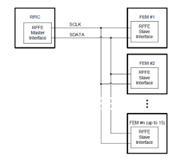
Figure 1. RFFE v1 Interface and Bus Structure
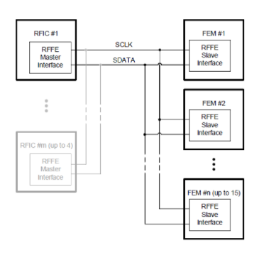
Figure 2. RFFE v2 interface and bus structure
RFFE Pin Descriptions:
VIO
VIO is the RFFE interface voltage reference or supply. The primary function of the VIO signal is to provide a shared voltage reference for the SCLK and SDATA pins for all devices on an RFFE bus instance.
SCLK
The SCLK signal provides the clocking and synchronization for all devices on an RFFE bus. It is always sourced by the Bus Owner Master (BOM) device.
In the case of a bus that has multiple master devices, the responsibility for the sourcing of SCLK is transferred to the new BOM any time that a master switchover occurs. There will be a dedicated SCLK signal for each RFFE bus instantiation.
SDATA
The SDATA signal on an RFFE bus provides the mechanism for command and data transfers, on the RFFE bus.
For write only slaves the SDATA pin is input-only. For slaves supporting read and write operations, the SDATA is bi-directional.
FREQUENCIES OF OPERATION: RFFE BUS SPEED RATES
RFFE provides a continuous range of frequencies for operation thus providing flexibility in clock sourcing. The active RFFE master device BOM is responsible for sourcing the non-continuous bus clock (SCLK) by specified requirements such as edge transition times.
The master device may select a desired operating frequency for SCLK at any time. The available range of SCLK frequencies and their parameters are given in the table below:
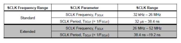
Figure 3. RFFE Frequencies of operation
RFFE Protocol: Data Transfer Structure
SEQUENCE START CONDITION (SSC)
The Sequence Start Condition (SSC) shall be a unique condition on the bus which is identified by a rising edge of SDATA, followed later by a falling edge on SDATA, all while SCLK remains at a logic ‘0’ level. The SSC is used by the master to identify the beginning of a new command sequence. Slaves shall synchronize themselves to expect a new command sequence following the detection of an SSC. The master shall generate the SSC by driving SDATA to logic level ‘1’ for one SCLK period, then to logic level ‘0’ for one SCLK period, all while holding SCLK at logic level ‘0’.
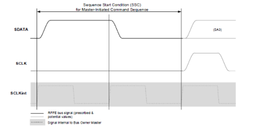
Figure 4. Sequence start condition
FRAMES
There are three types of frames and all three frame types consist of address plus command, or of data, or address bits, plus a parity bit.
COMMAND FRAME
A command frame shall consist of a 4-bit slave address field, an 8-bit command payload field, and a single parity bit, for a total of 13 bits. The first four bits of the address field are the slave address (SA) bits, followed by the eight command bits, and finally followed by the parity bit for the frame. The parity bit is calculated over the 12 bits of the CF. The command frame structure is shown
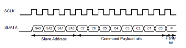
Figure 5. Command Frame
DATA OR ADDRESS FRAME
A data frame or an address frame shall consist of right data bits or eight address bits respectively and a single parity bit. The frame is called an address frame when the payload bits carry address information and a data frame when the payload bits carry data information. Otherwise, the frame structure is identical. The type of payload data being carried is defined by the position of the frame within the command sequence.
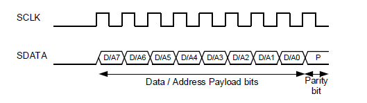
Figure 6. Data or Address Frame
NO RESPONSE FRAME
All bits including the parity bit of a no response frame (NRF) shall be ‘0’. This frame may be generated by driving SDATA to logic level ‘0’ or by passively allowing the master to pull SDATA to a logic ‘0’ for the duration of the frame. A no-response frame is nine bits long since it is a data frame. A no-response frame may be transmitted passively or actively. A passive no-response frame may be the result of a write-only slave during a read command sequence, while an active or passive NRF may be the response from a read-capable slave in the event of a read operation to an unused register location in that device.
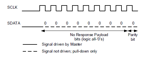
Figure 7. No Response Frame (Passive)
PARITY BIT
All frames shall end with a single parity bit. The parity bit shall be driven such that the total number of bits in the frame that are driven to logic level '1', including the parity bit, is odd, thus
achieving odd parity.
RFFE Protocol Debug:
Debugging RFFE Protocol continues to remain a challenge. Decoding the packets will help to better understand Protocol related issues and help speed up the engineering debug and development time. Prodigy has developed a Protocol Analyzer for debugging the RFFE protocol.
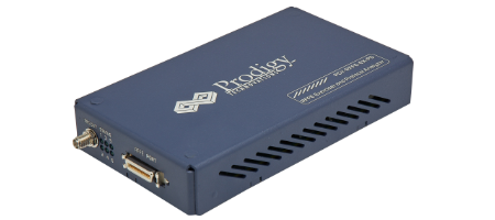
RFFE Protocol Analyzer and Exerciser
About Prodigy:
Prodigy Technovations is the leading provider of protocol analysis solutions. Prodigy has developed state of the art Protocol analyzer to debug various Protocols. The protocol analyzers range from CAN, I2C, SPI, QSPI, I3C, PCIe, and UFS Plus many other protocols on the serial bus.