eSPI Protocol INTRODUCTION
eSPI stands for the enhanced serial peripheral interface. It was developed by Intel. eSPI is an all-in-one bus that was designed to replace the LPC bus as well as the SPI bus, SMBus, and sideband signals. For designers of computing applications, migrating from the LPC bus to the eSPI bus offered benefits such as cost savings, lower voltage, simplified board layout and design, and low power consumption. The eSPI bus can either be shared with SPI devices to save pins or be separate from the SPI bus.
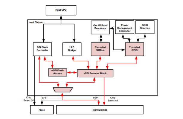
Figure 1. An EC/BMC/SIO connection over the eSPI bus
Sideband pin communications between the chipset and these devices are converted to in-band messages through the eSPI interface as part of the effort to reduce the component pin count and provide a migration path toward the elimination of high-voltage 3.3V I/O pins.
eSPI: BENEFITS
eSPI is defined to meet the following requirements.
● Medium Bandwidth: The bus bandwidth needs to be higher than that of the Low PinCount (LPC) bus.
● LPC Replacement: Supports all the capabilities needed to replace the parallel LPC interface. However, 8237 DMA and Firmware Hub (FWH) are not supported over this interface.
● Sideband Pins as In-Band Messaging: Facilitates the removal of sideband pins for communication between chipset and slave devices by converting this communication into in-band messages sent over the eSPI bus.
● Real-Time Flash Sharing: Supports flash sharing based on partition-able memory mapping. Allows real-time operational access by chipset and slave devices.
● Chipset and Slave Devices SMBus Replacement: Supports tunneling of all SMBus communication between chipset and slave devices over the new interface as in-band messages.
● Scalable bandwidth: Allows the bandwidth to be scaled based on application needs to optimize power versus performance. This could be done through frequency scaling or
varying the number of active data pins.
● Low Voltage I/O Buffer: eSPI uses the same I/O buffer as Serial Peripheral Interface (SPI). The I/O buffer will support only a 1.8V mode of operation for the eSPI bus.
eSPI Protocol: PIN DESCRIPTIONS
RESET
Reset is typically driven from eSPI master to eSPI slaves. In other configurations, the eSPI Reset could be generated by the eSPI master and thus, it is driven from the eSPI master to the eSPI slave.
CHIP SELECT
eSPI master and eSPI slaves must tri-state the interface pins when their respective eSPI Reset is asserted. The Chip Select and I/O[n:0] pins require weak pull-ups to be enabled on these pins.
SERIAL CLOCK
The direction of the serial clock is from master to slave. A serial clock provides the reference timing for all the serial input and output operations.
ALERT
The direction of Alert is from slave to master and it is asynchronous. Alert is used by eSPI slaves to request service from the eSPI master. The alert pin is optional for single master-single slave configuration.
I/O[n:0]
These are bi-directional input/output pins used to transfer data between masters and slaves. The value of ‘n’ may be 1 or 3 depending on the I/O mode.
In Single I/O mode (n=1), I/O[0] is the eSPI master output/eSPI slave input (MOSI) whereas I/O[1] is the eSPI master input/eSPI slave output (MISO).
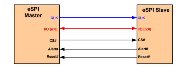
Figure 2. Single Master-Single Slave with eSPI Reset# from Slave to Master
eSPI Protocol: BUS TRANSACTIONS
The Serial Clock must be low at the assertion edge of the Chip Select while eSPI Reset has been de-asserted. The first data is launched from the master while the serial clock is still low and sampled on the first rising edge of the clock by the slave. Subsequent data is launched on the falling edge of the clock from the master and sampled on the rising edge of the clock by the slave. The data is launched from the slave on the falling edge of the clock. The master could implement a more flexible sampling scheme since it controls the clock. All transactions on eSPI must be in multiples of 8 bits.
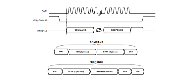
Figure 3. Basic eSPI Protocol
The eSPI transaction consists of a Command phase driven by the master, a Turn-Around (TAR) phase, and a Response phase driven by the slave. The Command phase consists of a CMD, an optional header (HDR), optional DATA, and a CRC. The Response phase consists of an RSP, an optional header (HDR), optional data, a Status, and a CRC. CRC generation is mandatory for all eSPI transactions where the CRC byte is always transmitted on the bus. However, CRC checking is default disabled after reset and it is enabled by SET CONFIGURATION. When CRC checking is disabled, the CRC byte is ignored by the receiver. A transaction could be initiated by the master through the assertion of Chip Select, Start the clock, and drive the command onto the data bus. The clock remains toggling until the complete response phase has been received from the slaves.
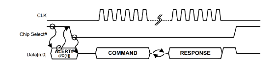
Figure 4. Slave Triggered Transaction (Single Slave)
A transaction could be initiated by the slave by first signaling an Alert event to the master. The Alert event could be signaled in two ways. In the Single MasterSingle Slave configuration, the I/O[1] pin could be used by the slave to indicate an Alert event. In the Single Master-Multiple Slaves configuration, a dedicated Alert pin is required. The Alert event can only be signaled by the slave when the slave’s Chip Select is high.
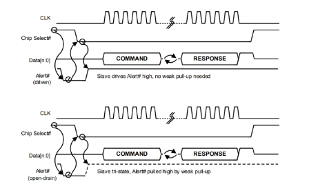
Figure 5. Slave Triggered Transaction (Multiple Slaves)
Debug of eSPI Protocol:
Debugging eSPI remains a challenge in engineering development. Prodigy Technovations provides state of an art tool for eSPI Protocol Debug and analysis.
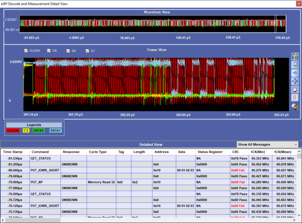
eSPI Electrical Validation and Protocol Decode Software
About Prodigy:
Prodigy Technovations continues to lead in the protocol analysis space. Prodigy Technnovation offers protocol analysis for basic serial protocol like I2C to complex high speed protocols like PCIe. The protocol analyzers range from CAN, I2C, SPI, QSPI, I3C, PCIe, and UFS Plus many other protocols on the serial bus.