I2S Protocol
I2S Protocol Introduction
Today’s digital systems – from the Digital TV in the living room, Alexa, and google home for playing music and switching from text-based search to voice-based search– are driving convergence on many fronts. Quality of Experience is taking center stage. Audio requirements in Computers, Mobile Handsets, and Home Automation products have changed dramatically. Audio content to and from the processors is increasingly becoming digital data.
I2S Standard: Theory of Operations
The digital audio signals in most systems are being processed by several devices, such as ADCs, DACs, DSPs, Digital I/O interfaces, and many more. To enhance flexibility and interoperability, it is critical to have standardized communication structures, for both the equipment and the silicon developers.
Inter-IC Sound (I2S) bus – a serial link, is developed especially for digital audio. The bus handles only audio data through a simple, 3-line serial bus consisting of:
• Continuous Serial Clock (SCK);
• Word Select (WS); and
• Serial Data (SD)
The Clock
The transmitter and receiver have the same clock signal for data transmission. Typically, the transmitter acts as the master and generates the bit clock, word-select signal, and data. The slave derives its internal clock signal from an external clock input. In complex systems having several transmitters and receivers, a system master controls digital audio data flow between various ICs.
For data and word-select inputs, the external to internal clock delay is of no consequence because it only lengthens the effective set-up time. The major part of the time margin is to accommodate the difference between the propagation delay of the transmitter, and the time required to set up the receiver.
All timing requirements are specified relative to the clock period or the minimum allowed clock period of a device. Thus, higher data rates can be used in the future.
Word Select
The word select line indicates the channel being transmitted:
• WS = 0; channel 1 (left);
• WS = 1; channel 2 (right).
In the slave, this signal is latched on the leading edge of the clock signal. The WS line changes one clock period before the MSB is transmitted. This allows the slave transmitter to derive synchronous timing of the serial data that will be set up for transmission. Moreover, it enables the receiver to store the previous word and clear the input for the next word.
Serial Data
I2S Protocol offers a very high degree of flexibility. The transmitter and receiver may have different word lengths. Also, the transmitter doesn’t need to know how many bits the receiver can handle, nor does the receiver need to know how many bits are being transmitted.
To enable this, the Serial Data is transmitted in two’s complements with the MSB first. The MSB has a fixed position, whereas the position of the LSB depends on the word length. When the system word length is greater than the transmitter word length, the word is truncated (LSB set to ‘0’) for data transmission. If the receiver gets more bits than its word length, the bits after the LSB are ignored. In case the receiver is sent fewer bits than its word length, the missing bits are set to zero internally.
Challenges in Debug I2S Protocol:
The key performance of current-generation digital Audio is measured based on the quality of output audio, battery life, and portability. To achieve these performance factors, the industry converts the analog audio signal into digital to reduce the effect of SNR and also employs multiple digital signal processing algorithms to create a compelling audio experience. To enhance the battery life, the designer pursued chips designed based on power-aware technology. This technology turns on and off the different blocks within an IC.
These design practices throw up the following challenges to designers.
• Debugging the content of the Audio Serial buses
• Ensuring physical layer timing and compliance with standard
• Ensure very high-level signal fidelity during the signal transformation from Analog to Digital and vice versa.
• Reducing the noise components generated due to mixed-signal design and new generation power-aware ICs.
• Interoperability of different vendors Audio subsystems
• Maximize the design margins with low power and voltage
Traditionally often, engineers use multiple instruments such as an Audio analyzer for dealing with audio domain-related challenges, a logic analyzer for dealing with link-layer challenges, and Oscilloscopes for dealing with signal integrity and timing challenges. Involving multiple instruments adds additional complexity to the test setup.
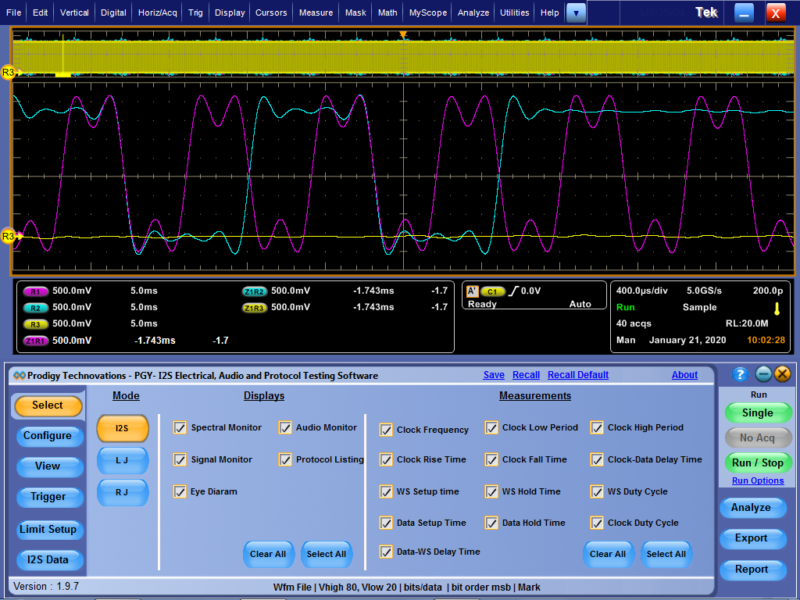
Now a single tool arrives to address all of the above challenges in the I2S protocol design. PGY-DAA I2S Digital Audio Analysis software along with the Tektronix Oscilloscope is a single tool to cross-examine the protocol layer and the PHY layer while verifying the audio performance and helps to address all the challenges listed above.
Summary
PGY-I2S I2S Audio / Protocol Decode / Electrical Test Software along with the Tektronix DPO7000, DPO/MSO70000/B series oscilloscope offers a comprehensive set of tools that enables design and validation engineers to efficiently, and effectively, debug the toughest I 2 S challenges.


