How does 5G impact UFS (Universal Flash Storage)?
What is UFS Protocol? What is its connection with 5G?
The arrival of 5G is changing the way the smartphone is being used and leading the way to the next generation of mobile technology. The smartphone vendors are planning to offer seamless and immersive experiences on mobile devices. 5G offers ultra-fast transfers, low latency, and low power consumption on mobile devices. These high-speed data transfers mandate the need for high-speed storage interfaces such as UFS 4.0/3.0 on mobile devices.
UFS stands for Universal Flash storage and offers more high-speed data processing than its predecessor, eMMC. This high-speed data transfer enables next-generation experiences such as 8K multimedia streaming and paves the way for augmented reality and Virtual reality experiences.
What does UFS 4.0 mean?
UFS 4.0 specification supports three new features:
- Write Booster: This is designed to increase write speeds by using a pseudo-SLC cache. Similar technology is already present with current-generation SSDs.
- Deep Sleep: The new lower power state designed for the UFS devices that use the same voltage regulators for storage and other functions.
- Performance Throttling Notification: This enables the UFS device to inform the host about performance throttling when overheating.
UFS 4.0 is the next-generation standard after UFS 2.0, UFS 3.1. UFS 4.0 has a very advanced capability to support 5G experiences. UFS 3.1 supports 128,256,512 GB of storage capacity. The data download capacity is up to 1200 MB offering gigabytes of sequential write speeds. UFS 3.1 also supports random read and random write of from 63000 to 68000 IOPS.
How to Debug UFS 4.0?
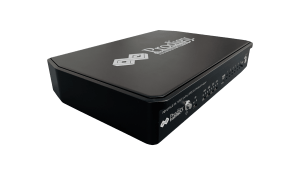
UFS 4.0 debugging is a challenge as it’s very high-speed data transfer. Prodigy offers state-of-the-art debug hardware to Debug UFS protocol.
UFS 4.0 Protocol Analyzer comes with the following features:
- Supports version MPHY 5.0, UniPro 2.0, and UFS v2.1/3.1/4.0
- Supports PWM G1 to G7 and HS G1, 2, 3, 4, 5 Rate A and B Series
- Supports one/two data lanes (2 TX and 2 RX)
- Flexibility to capture very large data using continuous streaming of Protocol data to host computer with 16GB Internal acquisition memory field upgradeable up to 64GB.
- Hardware-based resizable circular buffer with pre/post-trigger.
- Flexibility to decode selected data from a 16GB buffer.
- Solder down active probe provides high signal fidelity.
- Decoding at MPHY, UniPro, and UFS layers.
- Trigger-based on MPHY, UniPro, and UFS layers packet content.
- Trigger out a signal at the trigger event allows the triggering of other instruments such as an oscilloscope.
- Interface to host system using USB 3.0.
- Flexibility to upgrade the hardware firmware using the GbE interface provides easy field up-gradation of FPGA firmware.
- Decoded data packets can be exported to a text file for further analysis.
- Lightweight and can be deployed for on-site/ field tests.


