How did the AI Edge voice chip Company accelerate the Post Silicon bring up?
INTRODUCTION
A startup was working on AI Edge-based voice processor chip. The voice-based AI chip is designed to consume the lowest power as it’s used in consumer headphones or earbuds. The startup was about to tape out the chip and was preparing for a post-silicon bring-up. It faced very significant barriers in the development phase with I/O peripherals like I2C and SPI and using Prodigy protocol analyzer and exerciser it was able to quickly solve some challenges and get ready for the post-silicon validation. The older generation chip was done in 40nm and the latest migration after testing and getting the confidence was to migrate to a 7nm process node.
THE AI PROCESSOR
The AI processor is one of the first-generation chips that enables complete voice control for consumer products. The consumer devices can be smart speakers, remotes, earbuds, and automotive solutions. The AI processer does the inference and training to enable autonomous speech recognition without sending audio to the cloud for further processing.
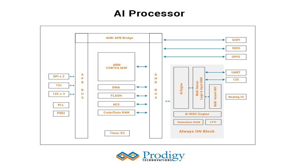
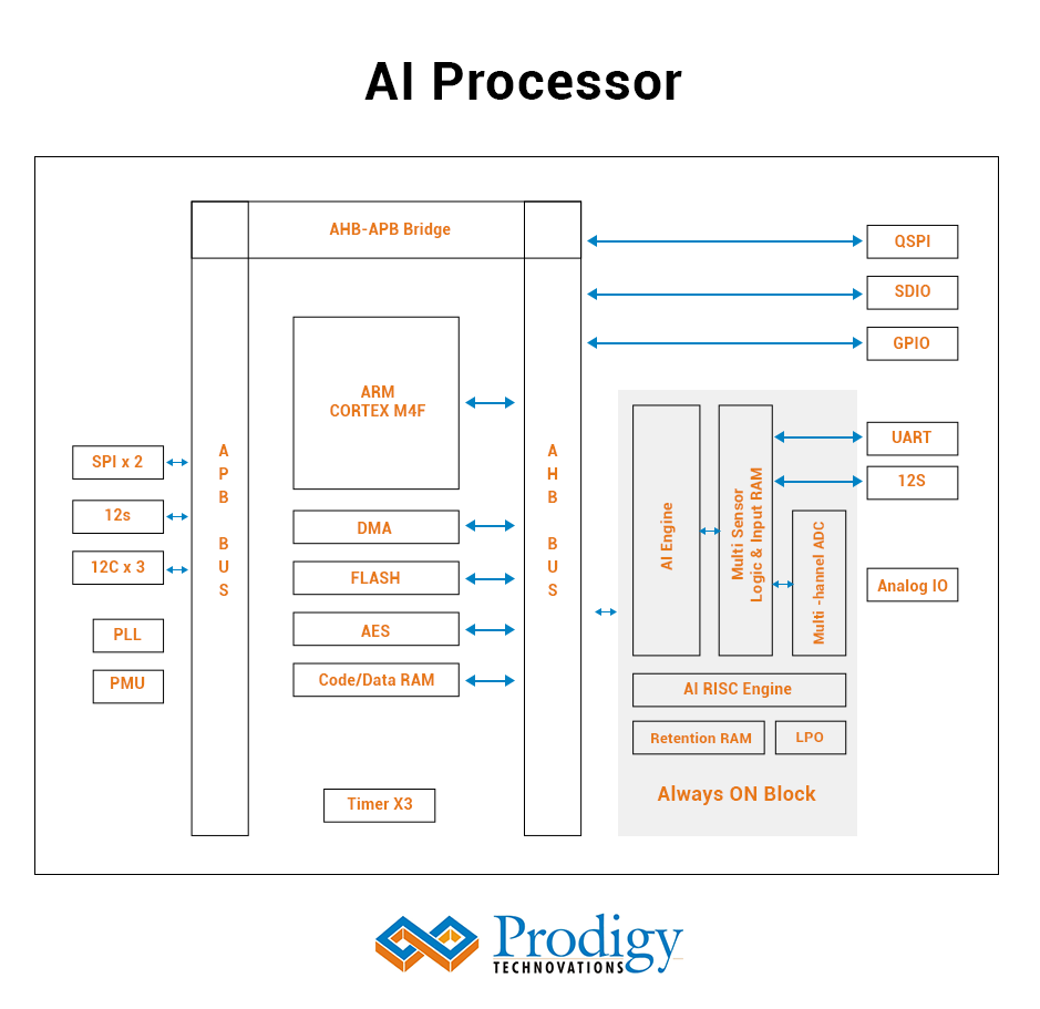
The AI Processor details are as follows:
Key Features:
- 5 AI cores provide 1028 MAC operations per clock cycle
- 60 uW active power consumption in inference tasks
- Sensor fusion with 8 I/Os
- Years of operations on a coin cell battery
- Ultra-low-power ADCs
- 5nm process node
Architecture Diagram :
Development Challenge
The startup was in the tape-out phase of its design when it approached Prodigy Technovations for solutions to help them verify the feasibility of its design. One of the major requirements was to help in testing their standard peripherals which would be used in conjunction with the AI processor using serial communication protocols like I2C, SPI, QSPI, and I2S. The peripherals in the picture were EEPROMs, SDIO’s, and FLASH memory which were being used in applications involving video processing and sensor fusion. The AI processor was to act as the master and the consecutive peripherals as slaves.
Hence, Prodigy’s I2C SPI Exerciser and Protocol analyzer proved to be a handy tool in debugging design issues and observing how the slaves behave under different test cases our product was capable of generating. In this case, the prodigy I2C SPI protocol analyzer would help with decoding the protocol bus and reporting and monitoring, and capturing any bus transaction-level issues.
Also, another requirement put forward was to be able to use the Prodigy I2C SPI Exerciser as a slave and their AI-based processor as a master, to observe different scenarios and do the timing control on bus signals and also improve any development issues on the peripheral during the post-silicon bring up.
Some of the key changes for SPI and I2C Protocol were
- Provision for BYTE timing delay and delay between transactions.
- Validation of Basic read and write test transactions and integration them via API into the development flow to automate testing
Problem Solved and Key Learnings
The slaves used were I2C Atmel and SPI Winbond. The read and write operations were not in a proper sequence. On investigation using the protocol analyzer and exerciser, it was found that the datasheets of the corresponding slaves were not referred to by the design team. The Prodigy protocol analyzer and exerciser were not only able to debug the issue but also gave the flexibility to figure out issues in the development team. Check out our protocol analyzer and exercisers.


