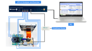
Universal Flash Storage (UFS) uses the MIPI Alliance’s MPHY physical layer specification to interconnect the UFS device with the host (SoC) or application processor. This is an embedded interface with no connectors between the host and UFS device. In typical electronic systems, the MPHY signals are routed between PCB layers, making them inaccessible. However, test and validation engineers need access to these signals for debugging UFS physical and protocol layers, making it challenging to debug UFS issues, often delaying time to market.
There are different phases in UFS product validation. The most common stages are:
- Pre-silicon validation
- Post-silicon validation
- Engineering and production validation
Each of these stages presents different challenges in accessing MPHY/UFS signals. Let’s explore the challenges and solutions offered by Prodigy Technovations.
a. Pre-Silicon Validation Phase
In this early phase of product development, SoC/AP developers validate the UFS controller on an emulation or prototyping platform using coaxial cables. A typical pre-silicon validation setup is as follows:
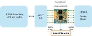
During testing, verification engineers need to monitor UFS protocol activity between the UFS host and device. However, it is difficult to tap the signals from coaxial cables connected via mSMP or SMA connectors. One effective solution is the power divider interposer. Here’s a typical validation setup using a power divider interposer:
The power divider interposer passively splits the signal between the UFS controller IP and the UFS device, providing access to the MPHY signals. These signals are then amplified for input to UFS 3.1/4.0 protocol analyzers. This solution allows validation engineers to monitor protocol activity effectively during the pre-silicon phase.
b. Post-Silicon Validation Phase
After the silicon is developed, semiconductor companies must ensure that every interface on the IC meets specifications. Protocol layer testing is critical to ensure that the device can operate reliably across different ICs and operating environments. To achieve this, post-silicon validation teams build platforms that provide access to signals for various test equipment, such as oscilloscopes and protocol analyzers.
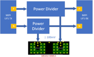
For UFS protocol validation, engineers develop a platform that simulates real-world use cases and provides signal access without compromising signal integrity. One method is integrating a power divider circuit in the validation platform, as shown below:
The MPHY signal is tapped and terminated to a miniSMP connector, which can be connected to the UFS 4.0 protocol analyzer. The power divider circuit ensures that the signal impedance matches MPHY specifications, minimizing signal integrity issues. Engineers can now easily connect the PGY-UFS4-PA UFS4 (23.32Gbps) Protocol Analyzer to the platform to validate UFS, UniPro, and MPHY protocol layers. When the analyzer is not in use, the miniSMP connector can be terminated with a 50-ohm block.
c. Accessing UFS Signals During Engineering and Production Validation
When developing a product for mass production, factors like board design cost, manufacturability, and space limitations must be considered. PCB real estate is often limited, making it difficult to access MPHY signals for UFS protocol debugging during development or post-sales failure analysis.
In cases where test pads are available, Prodigy Technovations offers solder-down probe tips that can be attached to these tiny test points. A typical use case is shown below:
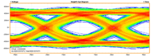
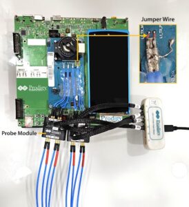 Using a short jumper wire (approximately 3mm), engineers can solder the probe tips to the test points. Although this setup may cause impedance discontinuity, the probe module compensates using a continuous time linear equalizer (CTLE) and amplifies the low-amplitude signals for analysis. The resulting eye diagram at the probe module output is shown here:
Often, access to UFS signals for debugging purposes is unavailable because the MPHY signals are routed between PCB layers due to limited real estate. A typical signal routing scenario is shown below.
 To overcome this challenge, Prodigy Technovations has developed an innovative Board-to-Board interposer solution. This solution consists of two PCBs: the bottom PCB, which is soldered in place of the UFS device in the system, and the top PCB, which accommodates the UFS 3.1/4 device in a socket and includes an mSMP connector to tap MPHY signals for UFS protocol analysis. The top and bottom PCBs are connected by a very short, high-speed differential cable. The UFS device can either draw power from the system or be powered externally. All signals required for UFS device operation are routed between the two PCBs, while signals for protocol analysis are passively tapped using a power divider circuit and probe module integrated into the top PCB.
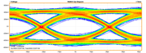
The probe module’s output is terminated at a miniSMP connector, allowing test and validation engineers to easily perform protocol analysis. The entire design is impedance-matched, ensuring signal integrity, and the eye diagram at the miniSMP connector demonstrates this performance.
A typical test setup for the Board-to-Board interposer solution is shown below.
In this setup, the miniSMP connector on the top PCB is connected to the UFS 4 Protocol Analyzer. The probe power module powers the active circuitry (CTLE and amplifier) on the top PCB, providing a reliable and straightforward method for UFS 3.1/4 protocol analysis.
Prodigy Technovations has successfully simplified the probing requirements at various stages of UFS product development and production. With over a decade of experience in providing UFS 2.1, UFS 3.1, and UFS 4.0 protocol analysis solutions, we understand the evolving market needs and have developed innovative probing solutions for various use cases. As a contributing member of the MIPI Alliance, we actively participate in the development of test solutions.


